14 Dec 2013

Hacking a Disco Ball - Part 1

Several months ago, one of my friends bought a cheap disco ball on ebay like this one. When plugged in the wall outlet, the disco ball turns and produce automatic lights pattern. After using it a couple times, he found the built-in pattern to be pretty boring so he asked me if it was possible to hack the electronics inside to create his own patterns.


We then opened the disco ball to see how it worked, the design was pretty simple. Inside the ball, there is 2 printed circuit board and a 120V motor. One of the PCB only contains 3 big LEDs for the red, green and blue color. On the side of the PCB you have a six pin connection that gives access to the 3 cathodes and 3 anodes of the LEDs.


On the other PCB, you have a transformer and 7805 regulator to provide low voltage for the LEDs and a couple chips for animating the hardware of the ball. Like most Chinese stuff I've seen, the controller PCB is very cheaply made and by looking at the quality of the soldering, I wonder how it can work properly.


To hack the disco ball, I suggested to my friend that we get rid of the controller board and make our own so we can control each LEDs and the motor. The content of the PCB is quite simple :

  • 5V input connector
  • 120V input connector
  • Microcontroller (I chose the Propeller from Parallax)
  • 3.3V voltage regulator
  • 3 MOSFET transistors to drive the LEDs
  • Triac to turn ON and OFF the 120V motor
  • Couples of connectors for LEDs, motor and programming
For the software part, I scratched my head a little bit... I wanted to make something simple so we could create several lighting patterns easily, without messing too much with the code. I ended up with designing a simple scripting language to control the LEDs and motors. The language also features looping construct for the animations. Here is what is needed for the software :

  • Specification for the disco scripting language
  • Computer program to send the script to the disco ball
    • Functions to read the script file and translate it to a binary form
    • Functions to send the binary file serially to the microcontroller
  • Microcontroller program to receive and interpret the binary program
  • Software routines for controlling the motor and switching/dimming the LEDs
Even if this project is simple, completing each task took me quite some time and the project is almost finished. At the moment, all the software part is working and I'm waiting for the PCB that I ordered from OSH Park to arrive. Take a look at the preview of the PCB I got :

Front side

Back side


In the next part of this article, I'll give you an overview of the software involved in this project.

13 Nov 2013

Led matrix graphical user interface on the RaspberryPi

Yesterday, I plugged into my Raspberry Pi a little i2c LED Matrix. I wrote Python class to interact with it but I tought it would be really interesting to toggle the matrix's LED with a graphical user interface on the Pi itself. This is exactly what I done and you can take a look at the result in the following Youtube video:


To connections between the matrix and the Pi are really simple, you just need to connect 4 signals directly together : GND, 3V3, DATA and CLK. There is no need for pull-up resistor on the i2c clock and data lines, I presume the Pi already have them. The display is designed for 5V but it works really well at 3.3V.

For using i2c on the Raspberry Pi, you need to make some little configurations and install the Python libraries. These steps are outlined on this Instructable tutorial.

You will also need the PyQt4 package, install it with:
sudo apt-get install python-qt4

The final Python script is listed below. The LedMatrix class is the i2c communication part of my program and MatrixWidget is the graphical user interface. The Qt windows part does essentially two things, it reacts to mouse press and draw an array of ellipse (the virtual LEDs).

If you have any questions with the code, just ask in the comments and I will be glad to help. Happy coding!

#!/usr/bin/env python
import sys
from smbus import SMBus
from PyQt4 import QtGui, QtCore

class LedMatrix():
    ADDRESS = 0x70
    OSCILLATOR_ON = 0x21
    BLINK_CMD = 0x80
    DISPLAY_ON = 0x01
    BLINK_2HZ = 0x01
    BLINK_1HZ = 0x02
    BLINK_HALFHZ = 0x03
    BRIGHTNESS_CMD = 0xE0
    POS_X = (128, 1, 2, 4, 8, 16, 32, 64)
    POSn_X = (127, 254, 253, 251, 247, 239, 223, 191)
    POS_Y = (7, 0, 1, 2, 3, 4, 5, 6)

    def __init__(self, blink=0, brightness=15):
        self.bus = SMBus(1) #device on i2c channel 1
        self.bus.write_byte(self.ADDRESS, self.OSCILLATOR_ON)
        self.bus.write_byte(self.ADDRESS, self.BLINK_CMD|self.DISPLAY_ON|(blink<<1))
        self.bus.write_byte(self.ADDRESS, self.BRIGHTNESS_CMD|brightness)
        self.clearBuffer()

    def setBrightness(self, brightness):
        self.bus.write_byte(self.ADDRESS, self.BRIGHTNESS_CMD|brightness)
        
    def setBlinkRate(self, blink):      
        self.bus.write_byte(self.ADDRESS, self.BLINK_CMD|self.DISPLAY_ON|(blink<<1))
    
    def setPixel(self, x, y, state):
        if state:
            self.buffer[self.POS_Y[y]]|=self.POS_X[x]
        else:
            self.buffer[self.POS_Y[y]]&=self.POSn_X[x]

    def clearBuffer(self):
        self.buffer = [0]*8
    
    def writeBuffer(self):
        data = []
        for row in self.buffer:
            data.append(0)
            data.append(row)
        self.bus.write_block_data(self.ADDRESS, 0x00, data)

class MatrixWidget(QtGui.QWidget):
    def __init__(self):
        super(MatrixWidget, self).__init__()     
        self.w=20
        self.setGeometry(300, 300, self.w*10, self.w*10)
        self.setWindowTitle('Led Matrix')
        self.clearPixelBuffer()
        self.setFixedSize(self.width(),self.height())
        self.leds = LedMatrix()
        self.show()

    def clearPixelBuffer(self):
        self.buffer = [[0 for _ in range(8)] for _ in range(8)]

    def mousePressEvent(self, QMouseEvent):
        x = QMouseEvent.pos().x()
        y = QMouseEvent.pos().y()
        x = x/self.w-1
        y = y/self.w-1
        if x==-1 or y==-1 or x==8 or y==8:
            self.clearPixelBuffer()
            self.update()
            self.leds.clearBuffer()
            self.leds.writeBuffer()
            return
        pixel = self.buffer[x][y]
        if pixel:
            self.leds.setPixel(x, y, False)
            self.buffer[x][y]=0
        else:
            self.leds.setPixel(x, y, True)
            self.buffer[x][y]=1        
        self.update()
        self.leds.writeBuffer()
    
    def paintEvent(self, e):
        qp = QtGui.QPainter()
        qp.begin(self)
        self.refresh(qp, e)
        qp.end()
    
    def drawLed(self, qp, x, y):
        state = self.buffer[x][y]
        if state:
            col = QtGui.QColor("#FFF71C") #bright yellow
        else:
            col = QtGui.QColor("#373511") #dark yellow
        qp.setPen(col)
        qp.setBrush(col)
        qp.drawEllipse(self.w+self.w*x,self.w+self.w*y,self.w-3,self.w-3)
           
    def refresh(self, qp, event):
        qp.setBrush(QtCore.Qt.black)
        qp.drawRect(event.rect())
        for y in range(8):
            for x in range(8):
                self.drawLed(qp, x, y)

if __name__=="__main__":
    app = QtGui.QApplication(sys.argv)
    ex = MatrixWidget()
    sys.exit(app.exec_())

3 Nov 2013

I'm back for the winter

Hi everyone, I suppose some of you noticed that I have been silent for a couple months now. I have been pretty this summer with work and sport. At the beginning of October, I also moved into my new house so I had to move my workbench and all my electronic stuff. That was a lot of work!

Even if I have not posted any blog post, I have been working on a side project with a friend from Spain, Arrizen. The project is about domotics and you can learn more about it on our project website : Koollaborate.

Here is an excerpt from the website describing the project :

This project is about creating a home network of autonomous little sensor/actuator node called ‘Motes’. The Mote is a generic pluggable module comprising a brain (µController) and a communication module. The Motes are slaves to a central controller. Motes with different µC will be designed; they will share code librairies and projects should compile and work on the different architectures.

The goal of this project is to provide a cheap module for home automation that you can program to your will and make it communicate information. It will help someone focus on the project he wants to do and not designing controllers board over and over.


Domotics is a subject that interests me a lot because it involves electricity, electronics, programming, human machine interface, communication protocols, internet, servers...

For an house to be intelligent, it needs to be able communicate information to you, even if you are not home. In the next article, I will show you how to use the Python programming language to send emails and text messages on your cellphone.

18 Jun 2013

Switching AC loads with the TRIAC

Often in electronics, you need to switch loads (motors, lights, solenoids...) ON and OFF from a microcontroller's pin or the output of a low-voltage electronic circuit. When you are working with DC sources, a transistor gets the job done : you supply a voltage at the base/gate pin and current will flow from a higher voltage source at the collector/drain pin to the emitter/source pin (for NPN/N-Channel depending if the transistor is Bipolar/MOSFET). The problem with the transistor solution is that its current flow cannot be reversed. It's alright in most situation, but that won't let you work with AC loads.

The two most common way to switch an AC load is to use a mechanical relay or a TRIAC. The relay is easy to use, but has the disadvantages of being slow and consuming a lot of current (to keep the coil energized). Due to the fact that the relay contacts are mechanical, they will also wear out over time and make switching noise. On the other hand, the TRIAC is a small solid-state device that can switch really fast, hence you can use it to dim lights, control motors speed and heating elements. In fact, the TRIAC is used in recent digital electronics thermostats to regulate the power of a heater.

TRIAC overview

The TRIAC is a 3-pin semiconductor device that can let current flow from his main terminals in either direction. Some people describe its behaviour similar to 2 thyristors in antiparallel configuration.


When choosing a TRIAC for your application, take a look at its absolute maximum electrical ratings. The peak voltage (not RMS) of your AC source must be lower than the allowed peak maximum off-state voltage of the TRIAC datasheet. For a 120VAC source, this datasheet value should be higher than 170 volts (Vrms * sqrt(2)). There is also the RMS on-state current and the non-repetitive peak on-state current. Usually, just ensure that the average current of your load is below the RMS on-state current written in the datasheet.

Triggering the TRIAC

To trigger a TRIAC (let current flow between T1 and T2) you need to send a pulse on the gate with respect to the T1 terminal. When you read about TRIAC theory, you can see there is 4 different triggering modes (the four quadrants). All this means is that you can send a positive/negative pulse on the gate while T2 is positive/negative with T1 as the reference. Anyway, you don't really have to care about that to try the following circuits.

Keep in mind that once triggered, a TRIAC will continue to conduct until the current between its terminal drop below its holding current that can be found in its datasheet (a couple of milliamps for small TRIACs). This means that it will stop conducting at the end of the AC cycle, when there is no more voltage difference between hot and neutral (zero crossing). However, if you put DC voltage across the TRIAC terminals, it will conduct indefinitely; or until you cut the wire/shut the power off :)

#1 - With a single AC source

If you want to test if a TRIAC works and mess around with it, this is a simple way to wire it as it only requires a single AC source. I don't really think this circuit is useful unless you want to turn on an AC load by pressing or flipping a switch.  


#2 - With a DC signal

Here's a more interesting way to trigger a TRIAC. With this configuration, you can use an external low voltage DC signal to control an AC load. You have to watch out with this circuit because you have to tie the neutral of your AC source with the ground of your DC subsystem. I would not recommend this configuration with costly development board to control the TRIAC. It is also possible that noise could be injected in analogs part of your circuits, resulting in poor performances (e.g. ADC, op-amps...).


#3 - With a phototriac (opto-isolator)

In my humble opinion, the best and safest way to trigger a TRIAC would be to use a phototriac. It consist of using a chip that isolate the DC part of your circuit from the AC part. If you look closely to the right part of the circuit, it is almost the same as the first configuration we saw instead that the switch has been replaced by another TRIAC. The other TRIAC (phototriac) is triggered by the photodiode that is coupled with it in the chip package. In short, you only have to turn on the photodiode and the main TRIAC will be conducting, thus providing current to your AC load.


There is two kind of phototriacs : the ones with zero crossing circuit and the ones who don't. Phototriacs like the MOC3041 and the MOC3062 have an internal protection circuit that will not let you switch the main TRIAC on until the AC voltage is at the beginning of its cycle. This will prevent you to put a high voltage (middle of cycle) directly on the load as it could create a high in-rush current or excessive electrical noise. Phototriacs like the MOC3023 does not have this kind of protection. In a lot of applications, you won't really care about that.

Conclusion

If you want to try the different configurations above, ensure your load current is okay with the maximum current through your TRIAC. For the triggering resistor, choose it so the current through the gate is above the gate trigger current in the datasheet, just use Ohm's law. Please experiment with caution if you use mains electricity. When I tested the circuits above, I used a small 1.5W 120VAC to 12VAC open frame transformer like the one below so I could put my finger in the circuit without fearing an electrical shock or burning down the house.


12 May 2013

Adjustable constant current source (1A@12V)

The goal with a voltage source is to supply a load with a constant voltage. However, if the impedance of the load varies, the load current will vary too. For some reasons, if you need a constant current through a load, you will need a current source. A current source will sense the current through a load and adjust the voltage across it to keep that current constant. Take a look at the standard sources symbol:


Constant current sources can be useful in different situations, like DC motor control. For a DC motor, the torque is proportional to its current; this means that we can effectively achieve constant torque control with a current source. Another example is battery charging, some of them require to be charged at a constant current rate. They are also convenient to supply a constant current to a load that is highly dependent to temperature.

I have been searching for a while for an adjustable current source circuit and I think the following one is quite simple and reliable. It works with a single operational amplifier in negative feedback configuration. I added a second op-amp to make a voltage comparator with the potentiometer. It's used to light up the orange LED to indicate when the potentiometer is over 80% turned on (that is, >0.8A when the current source is shorted); this helps me remind that the components may be hot! I also placed a green LED in series with the 12V voltage supply to indicate when the circuit is working.


Here is the principle of operation of the op-amp current source (only the upper op-amp is used for the source):


  • The 5k potentiometer (R4) let you feed the non-inverting input terminal (+) with a voltage from 0-12V
  • The op-amp in negative feedback tries to keep (by adjusting its output voltage) the voltage at the inverting (-) and non-inverting (+) terminal the same
  • The output terminal of the op-amp will automatically drive the base pin of the PNP transistor so that the voltage at its emitter pin will stay the same as the potentiometer voltage
  • The current sense resistor (R5) will see 12V minus the potentiometer voltage across it (VR5 = 12 - Vpot)
  • With ohm's law, you can easily find the current supplied (VR5 / 10)

The maximum current that will be supplied by the current source will be about 1.2A (12V / 10Ω). If we consider the voltage loss in the Darlington TIP107, it will be more around 1A. 

With a 10Ω current sense resistor, this circuit is rather inefficient (lot of power dissipated). The reason why I did it like that is because I wanted the circuit to be safe when shorted. Normally, the current sense resistor is much lower (about 10 times and up).

For fun, I soldered the circuit on a perforated board. The red and black binding post are the load terminals. The 12V is supplied to the little blue terminal block. The TIP107 is supposed to be able to carry 8A but I realized that even at 1A, it was getting awfully hot; i then decided to put an heatsink on its back. If you make a similar circuit, beware of the current sense resistor too! I burned one of my finger on it


On the picture above, the load terminals are shorted with an hidden wire. The IC in the center is the dual op-amp (OPA2241). The strange looking component is the power resistor (brown devil from Ohmite), it's in ceramic with a flame resistant coating. There is a lot of soldering under the perf board!


4 May 2013

Microprocessors part 2 - Instruction set and programming

The PicoBlaze is one of the simplest processor to program in assembly language. Thanks to its RISC (Reduced Instruction Set Computing) architecture. A RISC processor only have a few instructions (about 20 of them), compared to a CISC (Complex Instruction Set Computing) processor. Having less instructions means that they can be packed at a higher density (because of the opcode length), thus requiring a smaller program memory. Moreover, it's easier to learn!

The PicoBlaze has been created by Ken Chapman from Xilinx and you can find an excellent and comprehensive documentation on the processor from Xilinx's User Guide 129 (UG129). I suggest you get it now.

Instructions groups

Before doing some programming, let's talk a little bit about the purposes of the PicoBlaze instructions and group them by category.

Arithmetic

These instructions are used to make simple calculations. It is possible to use them in a loop to perform more complex operation like multiplication, division, square root, power... The carry (added C) variant is used to make calculations on numbers larger than a byte (255). These operations modify the processor flags, more on that in a moment.
  • ADD
  • ADDC
  • SUB
  • SUBC

Logic

These logic instructions are used to perform bitwise operations on two bytes. They are often used to set, clear or toggle bits. This is done with a technique called masking; I'll give you some example in a next article on microprocessors programming.
  • AND
  • OR
  • XOR

Bit manipulation

To perform operation at a bit level, it is often useful to shift (or rotate) the bits in a byte. Shifting to the left or right can be useful for multiplication or division by a multiple of 2 (see binary number mathematical property). Often, when doing IO or mathematical operations, the bits you want to manipulate are located at the wrong position in the byte; you can solve the problem with these instructions. There is a subtle difference between shifting and rotating. When rotating, the bit that is pushed out of the byte (either 1 or 0) is fed back at the empty position. While shifting, that pushed bit is lost and the empty position is replaced either by a 1 or 0, depending if you use S?1 or S?0, respectively. 
  • RL / SL0 / SL1
  • RR / SR0 / SR1

Testing

These two operation (especially COMP) are essential to create conditionals. But before, you need to understand the processor flags. In the PicoBlaze, there is 2 status flag bits, ZERO (Z) and CARRY (C). The ZERO flag bit is set when the result of the last operation is zero. The CARRY flag bit is used to indicate various conditions, often used to signal a overflow/underflow condition while adding or subtracting. Back to our instructions... COMPare is used like a dummy SUB operation. The two bytes are subtracted (result not written back): if the Z flag is set, the numbers were equal; if the C flag is set, we know which number was greater than the other. The TEST instruction is a bit less used. It works like a dummy AND, the two numbers are "ANDed" together. If the result is zero, the Z flag is set. If there is a odd number of 1 bit in the resulting byte, the C flag is set (this is used to check the parity).

  • COMP
  • TEST

Memory manipulation

The LOAD instruction is used to move a register/constant value in another register. The FETCH and STORE instruction are used respectively to get data from scratchpad RAM into a register and put a register value into the scratchpad RAM. These operations are useful because you can reserve RAM or register address for a certain purpose and often, you need to move data to/from them.
  • FETCH
  • STORE
  • LOAD

Program redirection

The last piece of the puzzle, program flow control. The CALL/RETurn statements are used to describe functions that are called multiple times during the program lifetime (examples: doing a complex mathematical operation or getting a scaled value from a sensor). The inner working if these two instruction is simple: when CALL is executed, the address of the next instruction is pushed on a special memory space called the stack. The program flow then branch to the function and execute it until the RET instruction is encountered; the return address is then popped from the stack into the program counter (remember? the register that hold the value of the address of the current instruction). The stack allow multiple CALL to be nested. The JUMP instruction is often used with conditionals, where some instructions can be skipped depending of the current Z and C flags value.
  • CALL
  • RET
  • JUMP

Hello, PicoBlaze!

Enough theory, let's run the IDE and write some code (very small executable file, download it here). If you are using Linux, it works well under Wine. More info is available on Mediatronix's website, the maker of the IDE.

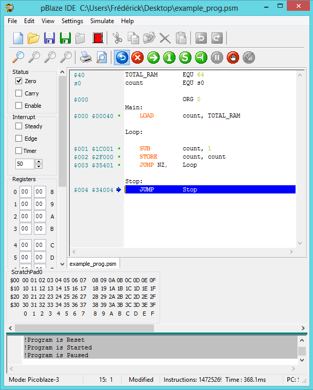
Our first PicoBlaze program will be simple and not really useful. Though it's great for learning purpose. We are going to write the number 0 to 63 in the 6-bit scratchpad RAM, backward! The picture below is the simulation result of the program (you can see the hexadecimal numbers in the ScratchPad0 debug area):


Before using the program, choose Picoblaze 3 in Settings (shortcut Ctrl+3). This is important! If you don't select this option, my sample code will not compile. Take a look in the bottom left corner of the window above, you should see Mode: Picoblaze-3.

The pBlazIDE is used to write the PicoBlaze program and simulate it in a convenient environment. When you open the IDE, you can either create a new project (Ctrl+N) and write the above program or just download mine and open it (Ctrl+O). When it's done, click the Assemble & Simulate (F12) button. The simulation mode is really cool because you can view the flags status, content of the registers, scratchpad memory, IO, etc... When you are in simulation, run (F9) the program, then pause it with the red button at the right (the one at the left is used to reset the simulation). You should be able to see the content of the ScratchPad0 area filled up.

Let's review the code line by line:
  1. The EQU keyword is used to assign a name to a register/constant value (this is optional). The TOTAL_RAM label will be used to represent the decimal value 64 (the total number of RAM register address).
  2. The register s0 will be used to store the count from 64 to 0. Let's name it that way.
  3. The ORG keyword is used to select the starting address of the following instructions. We put our program at the beginning of the program memory (address 0).
  4. The keywords followed by a colon are called label. It is conventional to name the address of our first instruction (Main:).
  5. The LOAD instruction is used to move a value into a register. In this case, we move 64 in the s0 register. Instead of using the EQU directive, we could have explicitly written LOAD s0, 64.
  6. The Loop: label is used to reference the address of the SUB and following instructions that we will repeat 64 times in a loop.
  7. Each time we go through the loop, we subtract 1 from the count register (s0). When the result of the subtraction will be 0, the Z flag will be set.
  8. We want to fill the RAM so we store the count value at the count address with the STORE instruction. The first time 63 (3F) will be written at address 63 (3F). At the end, 0 will be written at address 0. This is why it counts backward :)
  9. While the Z flag is not set, the JUMP NZ, will go back to the Loop label address. When the SUB instruction result will update the Z flag, this JUMP instruction won't be executed. Read the instruction like it were JUMP (if) NotZero.
  10. The two following lines are used to create an infinite loop that JUMP on itself. In a real life situation it is important to stop the execution of the program in a certain way because it will continue to execute the bits in memory in a unpredictable way.
Please note that I changed the color setting of the IDE syntax. In the picture above, there is 5 orange instructions (LOAD, SUB, STORE, JUMP, JUMP). These instructions are what is written in the program memory. Everything else is directives and labels. Once assembled with the pBlazASM.exe utility (you can find it on the website mentioned above), the binary that goes into the program memory is reduced to (in hexadecimal):

00040
1C001
2F000
35401
34004

Conclusion

I hope that you found this article interesting and you learned new stuff. I would like that you guys try to create a simple program or modify mine (using information in UG129) and play around with the IDE. Send me your experiments on my email address: fred_blais5(at)hotmail.com and I would be glad to showcase some of your programs in a next article. Also, don't hesitate to write programming ideas in the comment section, I'm all ears!


20 Apr 2013

Microprocessors part 1 - Introduction

The microprocessor has evolved a lot in the past 40 years since its debut in November 1971, with the Intel 4004 chip. Nowadays, we have a huge amount of different processing units to do electronics, control systems, robotics, etc...

The microprocessor can be seen has a large electrical circuit that can be serve a lot of different purposes and that needs to be supplied with a "binary file" of instructions to execute. The piece of silicon that doesn't change (microprocessor) is called hardware. The supplied binary code is called the software. By definition, hardware is fixed and software can be modified (with programming). I want to emphasize that point because I'll come back to that when discussing soft-core and hard-core in a FPGA. Throughout this article, I'll give practical examples with the PicoBlaze processor, which is a very simple soft processor core.

Computer bus

A bus in computing can be seen as a kind of highway for data. This highway can have several lanes (parallel bus) or the cars can line up one after the other (serial bus). This highway connects the different sub-systems of the computer. To show you the importance of device interconnect/communication here are some examples of common wired interface:

Peripheral

  • USB (Universal Serial Bus)
  • RS-232
  • FireWire
  • Thunderbolt

Printed circuit board

  • I²C (Inter-Integrated Circuit)
  • SPI (Serial Peripheral Interface)
  • 1-Wire
  • PCI (Peripheral Component Interconnect)
  • AGP (Accelerated Graphics Port)

Network

  • Ethernet
  • CAN (Controller Area Network)
  • RS-485

Video

  • VGA (Video Graphics Array)
  • HDMI (High-Definition Multimedia Interface)
  • DVI (Digital Visual Interface)

Hard drive

  • SATA (Serial Advanced Technology Attachment) 
  • IDE (Integrated Drive Electronics)

Internal IC buses

Even more important for today discussion, there is a lot of different buses inside integrated circuits to connect the different memories/caches to the processing unit and the inputs/outputs.

Program memory

The program memory is where the microprocessor program instructions are stored. This memory has a fixed width that matches the computer instruction width. It is sometimes considered as a ROM (Read-only Memory) because the program storage don't change while the processor is running. Here is an excerpt of the 18-bit PicoBlaze instruction set; that is, available instructions opcode understood by the processing unit.


Data memory

The data memory is used to store temporary data/variables. This kind of memory is also called the RAM (Random-Access Memory). You can see it like a kind of scratchpad area, where you can make some calculations on it and retrieve it later for other uses. Some CPU can process RAM directly, some others using the Load/Store Architecture have to switch this data back and forth in their internal registers to process it.

Harvard versus Von Neumann architecture

There is basically two kind of architecture to access memories. The Harvard architecture can access the program and data memory independently because it has two distinct buses to access them. In the Von Neumann architecture, the program and data memories share a single datapath. With a single memory bus, the processor will be less complex, but will also be slower than with separate buses. The Harvard architecture is mainstream now because of the Von Neumann Bottleneck.

CPU

The CPU (Central Processing Unit) is where everything is processed in a computer. Let's take a look at the internals schematics of the 8-bit PicoBlaze core:


At the top-left corner, there is the program memory. In this case, it's limited to 1024 18-bit instructions. The next block at the right is a small 10-bit pointer register called the PC (Program Counter). It is used to store the address of the next instruction to be executed. It can address all the 1024 instruction because it is 10 bits wide (2^10=1024). In the PicoBlaze, there's a quite small amount of RAM, only 64 bytes. There is however 16 registers that you can use for general purposes.

The CPU specific components in this schematics are the registers, PC, instruction decoder, buses and the ALU (Arithmetic Logic Unit). The ALU is the heart of the CPU, it's used to process the data that are brought to it by the different buses. You can see that it has 2 input buses and one output bus that work in conjunction with the registers. Everything that has to be processed has to be in the registers and is stored back in the registers. That it why it's a Load/Store Architecture core, there is no direct access between the ALU and the RAM. By the way, that PicoBlaze has a separate bus for instructions and data (as you can see above), so it's an Harvard processor.

The big arrows at the far left and right of the schematic is the interrupt line and the IO. It is what allow the PicoBlaze to talk and interact with the external world, like sensors and actuators.

MCU (µC)

A last thing I would like to discuss about is MCUs (Microcontroller Unit). A microcontroller contains all we've talked about previously on a single chip. They are mostly used in embedded systems, where they do  repetitive tasks in a reliable way.

In contrast, personal computers have a motherboard with separate components : CPU, GPU, RAM, hard drives, etc. They have much larger memories and faster clock frequencies.

The advantages of µC are their low cost and small power consumption. They're all around and you don't even see them; watches, Bluetooth headset, keyboard/mouse, microwave oven, remote control, digital photo frame, radio...

Conclusion

In the next part of this article, I'll write a little tutorial on PicoBlaze ASM programming and you will be able to simulate it on your computer!

14 Apr 2013

Digital Systems Part 4 - Decoder for 7-segment display

In one of my latest post about digital systems, I talked about the different types of combinational circuits. Let's take some time to discuss about the decoder and one of it's most widely known utilization: driving a seven segment display.

The seven-segment display


It is likely that you've already seen a 7-segment in a numeric watch or clock. This device contain 7 LEDs (hence 7-segment) enclosed in a small plastic case. It is generally used to display decimal digits from 0 to 9 (and display hexadecimal digit A to F). There are also some version of the 7-segment that contain a decimal point LED.

Being a 7-bit device, the 7-segment can display 128 (2^7) different "symbols". Take a look at this chart that shows all the possible combinations :


Driving the display with a decoder

The fact is that we don't really need all these combinations. We can then cut down 3 bits and have 16 (2^4) possible patterns, enough to hold the numbers 0 to 9. This is the goal of the 4 bit in, 7 bin out decoder as shown below :


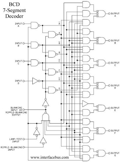
In the picture, you can read the term BCD (Binary Coded Decimal) that means a 4-bit code representing the decimal digit coded in binary (as the name imply). The BCD to seven-segment decoder can be implemented with simple logic gates (see picture below).


The CD4511 to the rescue

I already implemented a 7-segment display decoder with 74 series logic gates when I was in college and it was quite a challenge to get it working (without doing any wiring mistakes)! Integrated circuits like the CD4511 does the same thing, but in a tiny DIP package. Here is the basic schematic of a circuit using the decoder :


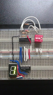
The "Lamp test" pin is used to light all the LED on the seven-segment to check if it's working properly. The "Blanking" pin does the opposite, it blanks the display. These two pins can be tied to the positive power rail as they are rarely used. The "Latch enable" pin, when pulled down to the ground, refresh the display with the current input (A0 to A3). The wiring is pretty straightforward, below is two pictures of what it looks like on a breadboard :


The CD4511 in action

There is multiple way to drive a decoder. It can be with simple DIP switches, or driven by a microcontroller. In the second video, I use 4 outputs of the Parallax Propeller to drive the chip. In the program I made, the delay between the counts is randomized between 150-1000 ms so the result is a bit more interesting...


13 Apr 2013

The op-amp as a comparator : temperature change detection circuit

In this post, we're going to take a brief look at one way of using an operational amplifier. To test the op-amp as a comparator, we will build a small and simple working circuit. Before diving in, let's take a moment to discuss about the operational amplifier.

Operational amplifier theory

The operational amplifier is a type of amplifier that can be use in a lot of different arrangements to create filters, comparators, integrators, inverting/non-inverting amplifiers etc... In the picture below, you can see the schematic representation of an op-amp and it's different terminals.


As you can see, it needs a positive and negative power supply. The op-amp has an electrical caracteristic called the open-loop gain. This gain is really high and usually range from 100,000@1,000,000. In open-loop, the relation between the output and inputs is dictated by this formula :


It is important to remember that the voltage on the output pin can only swing between the positive and negative supply voltage.

Op-amps are packaged into chips. It's possible that there are multiple op-amps in the same chip. Here is the pinout of the CA3140 IC :


Comparator mode

The principle of operation of the comparator mode is quite simple. In the equation, if the result of the substraction in the parenthesis is positive, the output will equal the positive supply (because of the high open-loop gain). If it's negative, the output will be limited to the negative supply, ground in most of applications. Briefly said (with a LED connected at the output) if V+ is at an higher voltage than V- the LED will be on.

Single supply (rail-to-rail) vs. dual supply

Most op-amp cannot drive it's output signal to their supply, only close to. If you want the output to go completely from a supply to the other, you need to order a rail-to-rail op-amp. These ones can be a little bit pricier. Let's take a look at the internal of a cheap dual supply op-amp that I purchased from Tayda Electronics.


I highlighted in red the components that limit the output pin from going all the way to the supply pins voltage. In the upper part, you have a diode (D7) with a forward drop of 0.7 volt and a transistor (Q18) that will saturate at 0.2-0.3 volt. This means that we cannot go higher than about 1 volt below the positive supply rail. For the negative supply, the transistors (Q15&Q16) will limit the voltage from going lower than 0.2-0.3 volt if the negative pin is tied to ground. By example, if we connect an op-amp to a 12 volt supply source, it's outuput will swing from 0.3 to 11 volts.

The temperature detect circuit


To demonstrate the comparator mode of an operational amplifier, I made a little circuit that use a thermistor. It detects a change of temperature above the ambient room temperature. Take a look at the schematic :


The thermistor is a resistance that is varying with the temperature. At the room temperature, the measured resistance is about 10kΩ, but when I touch it with my finger, it rapidly drop to 7kΩ. The 10kΩ fixed resistor in series with the thermistor make a voltage divider.

At ambient temperature, there is 6 volts at the voltage divider but when I touch the thermistor, the voltage goes a little bit below 5 volts. The output of the voltage divider is brought to the inverting input (-) of the op-amp. I want to compare this to 5 volts, so I used a 5V voltage regulator at the non-inverting input (+) (I was too lazy to make a 5V voltage divider from resistors). When I touch the thermistor with my finger, the (+) pin voltage is above the (-) pin voltage so the output goes almost to the positive supply. This cause the LED to light. (I changed the LED for a green one because the other one was too bright for the camera)


Conclusion

The principle of operation of this circuit can be transposed to a lot of different sensors or output device. It could have been a photoresistor (light detector) in place of the thermistor. We also could have replaced the LED by a fan so it could cool a hot device. Except for using an operational amplifier as a comparator, we rarely use it in open-loop (without any feedback). In a few articles, we'll take a look at other useful examples of circuits that uses an op-amp. 

24 Mar 2013

Milestones in digital electronics evolution

Ask someone about what electronics is, the answer will probably be related to all the modern devices we're using everyday : mp3 players, televisions, computers, cell phones... All of these are made of many integrated circuits containing millions of transistors (sized in nanometer). In numeric circuits, you always need a switching device that can be used to create logic gates and registers. However, these switches have not always been as small as they are today. Here are some milestones in the advances of modern electronics.

The mechanical relay (1835)

The relay is one of the oldest device used to make computers (primitive ones) and is still used a lot nowadays in all sort of different applications. The basic relay consist of a coil, spring, armature and contacts. When the coil is energized the armature close the normally open contact, otherwise the spring maintains the normally closed contact.


Computer with limited programming capabilities could be made using relays, like the Z1 in germany around 1938. It is considered as the first freely programmable computer, but it's operation was unreliable.


The vacuum tube (1907)

The vacuum tube is a great improvement over the mechanical relay because it contains no moving parts, that means it's a lot more reliable. Like the transistor, the vacuum tube can be used as an amplification device or as a switch. Hi-fidelity audio equipment still use vacuum tubes, for the clarity of the sound it provides. However, it is no more used as a switching device.


The first computers using vacuum tubes appeared around 1945 : the Colossus and the ENIAC. They were quite power hungry and heavy machines. The ENIAC contained around 17500 vacuum tubes as well as 1500 relays.


The transistor (1954)

The transistor is the device of choice to create digital electronics circuit and has evolved considerably since it's beginnings. The biggest advantages of the transistor over the vacuum tube is it's small size and small power consumption. That marks the debut of lightweight and portable electronics. In the picture below, you can see a replica of the first bipolar junction germanium transistor.


With the invent of the transistor, computers got a lot smaller and were ready to be manufactured for the commercial market. The IBM 608 is one of these fully transistorised computers. Below, a picture of Harwell CADET computer.


The integrated circuit (1962)

Transistors really began to get small when packaged into chips. That way, a lot of transistors could be packed on the same "die". I bet you have ever heard about Moore's law, stating in 1965 that the transistors count in integrated circuits will double every year for at least ten years. Here is a picture (a little bit outdated) representing the advances in the number of transistor in IC.

As you can see, the first generation of integrated circuits were used to make logic gates. Lots of things could be done with simple TTL gates, take a look at this circuit schematic of an arcade machine Pong game made by Atari in 1974.


 Generations of computers

I found an interesting article about computer generations here's the summary (mechanical relay computers not included) :
  1. First Generation (1940-1956) Vacuum Tubes
  2. Second Generation (1956-1963) Transistors
  3. Third Generation (1964-1971) Integrated Circuits
  4. Fourth Generation (1971-Present) Microprocessors
I bet you learned something new about computers... That's all for today folks!

23 Mar 2013

Serial and parallel I/O : shift registers

Sequential logic

When I discussed about digital logic, I mostly focused on combinational logic (decoders, adders...) but there is another really important type of digital circuits : sequential logic circuits. Sequential logic circuits are circuits that the outputs not only depend on the inputs, but also of the order in time that these inputs are read. Some new terms are introduced in this circuit type.

First of all, the concept of the memory bit : if the sequential circuit is time dependent, it means that there is some way to memorize the internal state of the circuit at a given time period. This is done with bistable circuits called latches or flip-flop (more on this in another article) that can be used as storage elements. If we combine more than one of these memory bits together, we can create registers.

Most of the time, sequential circuits work with a clock signal. A clock signal is a stream of square wave pulses that is used to synchronize the circuits. With the clock signal, data can be serialized on a single wire. This is the basis of high-speed computer buses. Here is examples waveform of a I2C bus transaction. The SDA signal is serial data and the SCL signal means serial clock and is square wave signal. The data being transferred is something like 011011001...


Shift registers

An interesting sequential logic device is the shift register. The shift register is a clocked device and can work in many modes. In the picture below, the blue cubes are memory bits and red arrows represent data being shifted right each clock cycle. Data can be shifted at the rising or falling edge of the clock pulses (depending on the IC). As you can see, inputs can be serial or parallel and outputs can also be serial or parallel. We're going to see two example of chips using a shift register.


Serial to parallel with the 74HC595 IC

The 74HC595 chip is often called an outputs expander. This is due to the fact that a µC (microcontroller) or other devices that can talk serially to this chip have the possibility to add a few output lines to their I/O. Has you may have already guessed, this IC is a serial input, parallel output shift register. With a single 595, you can add 8 output lines with as few as 3 wires. What's interesting is that you can daisy chain multiple 595 to add 16, 24, 32 and more outputs with only 3 control wires.

To be able to understand the inner working of that chip, I used it's datasheet. Below are some information that I found concerning the pin-out of the chip and the pins functionality.


The interesting pins are the 8 parallel outputs (Q0-Q7) and the 3 control pins : STCP (latch), SHCP (clock), DS (serial input). The OE pin is the output enable and must be tied to the ground to activate the outputs. MR is the master reset, tie it to Vcc (positive supply voltage) to get the chip out of the reset state.


In the table below, you can easily see what is going to happen with a given set of inputs. To make that short, a rising edge on the clock pin (SHCP) will store the serial input bit (DS) in the least significant bit (Q0S) of the shift register. All the previous bits in the shift register will move one bit toward the most significant bit (Q7S) one clock at a time. When the latch input is pulsed (STCP) the actual content of the shift register will be saved in the storage register. The storage register is directly tied to the parallel output (Q0-Q7). Remember that you must activate OE to make the outputs visible.


I wrote a driver in SPIN (the language used by my favorite µC, the P8X32A) to drive the 74HC595. I hope that in a couple of article I can write some tutorials about microcontroller programming. If you are a bit familiar with programming languages and algorithm, you should easily understand the code below.


You can see the result of the code on a LED bar-graph. On the first picture, $FF (1111_1111) was sent to the 595. On the second one, $55 was sent (0101_0101), can you see it? Please note that the 595 only has 8 output, so I only use 8 of the ten available LED on the bar-graph. Besides, I burned these two LEDs by doing some experiments on the bar-graph without current limiting resistors, duh!


Parallel to serial with the 74HC165 IC

The 165 IC is a parallel input, serial output shift register. Almost everyone has already used a device containing a 8 bit parallel to serial static shift register, if you ever played with an old Nintendo Entertainment System :)


In fact, this is the kind of chip used to store the 8 NES controller buttons (start, select, A, B, up, down, left, right) state and send it serially to the console. This operation is performed several times in a second. This can be seen as the inverse operation of the 595, as an input pins expander.

The working principle is quite simple : when PL (parallel load) is asserted, data from (D0-D7) are loaded in the shift register. After that, the bits are sent serially to Q7 (serial output from last stage) on each rising CP pin (clock) pulses.


I think that this IC is a little less interesting to demonstrate, as the data end up in the microcontroller and cannot really be seen... Though, it could be interesting to make some kind of gamepad with this IC as a demonstration. Moreover, the development board that I use has 2 NES gamepad port on it. Here is the source code for dealing with two gamepads (thanks to XGameStation, the developers of the board) :


Still here? :)

There was a lot of new information in this post, I did my best to make it the clearer and easier to understand as possible. For the lines of code shown, as I said, I will blog about programming later but there is a lot of interesting things to see before delving into that. Do not hesitate to write suggestions in the comment box!